Articles in this Volume

Research Article Open Access
Microwave Link Budget, Rain Attenuation, and the Role of Satellite Laser Communications in Future Networks
Article thumbnail
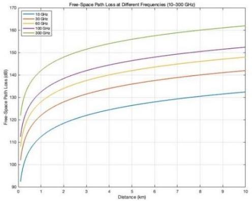
Microwave and millimeter-wave backhaul links play a vital role in modern communication networks by enabling high-capacity data transmission over distances ranging from hundreds of meters to several kilometers. These systems typically operate in high-frequency bands above 10 GHz, where a wider bandwidth is available. While such frequencies support compact antenna design and reduced interference through highly directional beams, they are also more susceptible to propagation losses and atmospheric effects, particularly rain attenuation. This paper presents a systematic analysis of microwave link budget design and rain attenuation mechanisms. Fundamental link budget calculation methods are introduced based on free-space propagation models, along with key system gain and loss factors. Rain attenuation is examined through established modeling approaches, and its impact on link reliability is analyzed under different environmental conditions. In addition, regional characteristics and advanced applications, including rainfall inversion and radar correction, are discussed to demonstrate the broader relevance of microwave link analysis. Furthermore, the study explores satellite laser communication as an emerging complementary technology. Compared with conventional microwave systems, laser communication offers significantly higher data rates, larger bandwidth, and enhanced security. However, it is more sensitive to atmospheric conditions. Therefore, a hybrid communication framework combining microwave and laser technologies is considered to improve overall system robustness and performance. The results indicate that accurate link budget modeling and effective mitigation of rain attenuation are essential for reliable high-frequency communication. Moreover, the integration of microwave and laser communication technologies is expected to play a key role in future satellite-terrestrial networks, particularly in the development of 6G systems.
Show more
Read Article PDF
Cite
Research Article Open Access
Analysis of Relationship Between the Rate of Temperature Change of Heat-Conductive Metal and the Velocity of Fluid Through Convective Heat Transfer Process
Article thumbnail
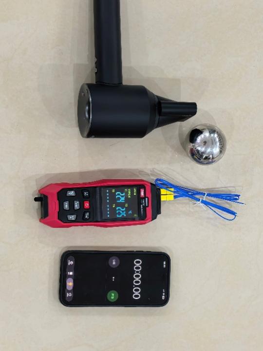
Heat transfer-related theories are crucial in practical engineering manufacturing processes, particularly in designing heating system and mechanical structures. This paper explores how convective heat transfer and fluid dynamics could be specifically related by demonstrating the proportional relation between the velocity of moving fluid and the rate of change in temperature of heat-conductive metal as the result of the heat effect by the fluid. A theoretical model for velocity-dependent expression is developed based on Nusselt, Reynolds and Prandtl's number, associated with Newton's Law of Cooling. An experiment is conducted using a hair dryer with different air speed settings, which are applied to a hollow stainless-steel metal ball, with 3 trials of data completed and recorded by a K-type thermocouple. The result demonstrates that higher fluid velocity leads to faster change in rate of temperature. This paper provides fundamental knowledge for engineering designs and applications like heat exchange systems and material selections for metal components.
Show more
Read Article PDF
Cite
Research Article Open Access
Structural Response and Thickness Sensitivity Analysis of a Dual-Panel CubeSat Solar Array under Different Incident Flow Angles in Low Earth Orbit
Article thumbnail
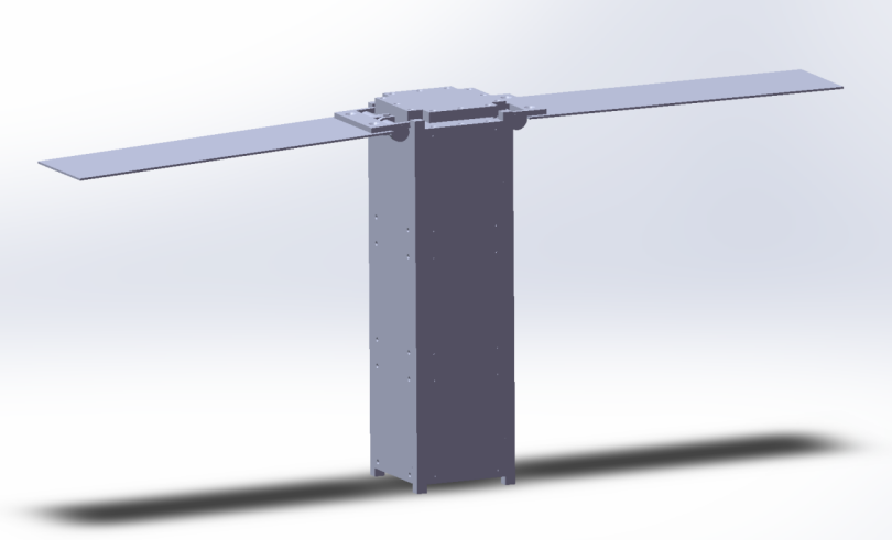
This study investigates the structural response of a dual-panel CubeSat solar array under different deployment angles in low Earth orbit. Deployable solar arrays are critical components for CubeSats and must maintain sufficient structural integrity under rarefied aerodynamic loading conditions. A simplified three-dimensional model is developed in SolidWorks, and finite element analysis is carried out using ANSYS Mechanical. The aerodynamic load at approximately 400 km altitude is simplified as an equivalent static pressure, and five deployment angles together with four panel thickness values are considered in a parametric study. The structural performance is evaluated in terms of von Mises stress. The results show that the deployment angle has a significant influence on structural response, with the fully deployed configuration identified as the most critical case. In addition, increasing panel thickness effectively improves structural stiffness and reduces deformation and stress. The findings provide preliminary design guidance for CubeSat solar array structures in low Earth orbit.
Show more
Read Article PDF
Cite
Research Article Open Access
Material Advantages and Device Challenges of Ag₂Se Quantum Dots for Near-Infrared QLED Applications
Article thumbnail
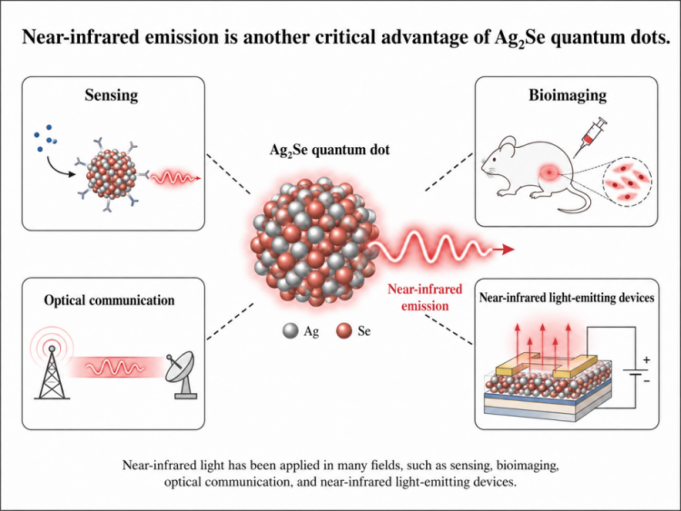
Near-infrared quantum-dot light-emitting diodes (NIR QLEDs) are being investigated for applications such as optical communication, sensing, imaging, and emerging display technologies. However, many established near-infrared quantum dots, such as CdSe- and PbS-based materials, or other heavy-metal-containing materials. Their toxicity presents an important obstacle to large-scale manufacturing, disposal, and commercial use. Ag₂Se quantum dots offer a possible alternative. They have several attractive features for near-infrared optoelectronic devices, including a narrow bandgap, near-infrared emission, and compatibility with solution-based processing. However, these material advantages have not yet been fully translated into high-performance NIR QLEDs. At present, the development of Ag₂Se-based NIR QLEDs is still at an early stage, mainly because device performance is affected by several issues, such as surface defects, non-radiative recombination, insulating long-chain ligands, imbalanced charge injection, poor film quality, and limited operational stability. This work reviews the principal material advantages of Ag₂Se quantum dots and discusses the major challenges associated with their integration into NIR QLEDs. Potential improvement strategies, including surface passivation, ligand exchange, carrier-transport-layer optimization, interface engineering, and device encapsulation, are also evaluated. Overall, Ag₂Se QDs have considerable promise for lower-toxicity NIR light-emitting devices. However, further progress in synthesis reproducibility, film formation, and operational stability is still needed.
Show more
Read Article PDF
Cite
Research Article Open Access
Carrier Transport and Recombination Mechanisms in PN Junctions and Applications in Semiconductor Optoelectronic Devices
Article thumbnail
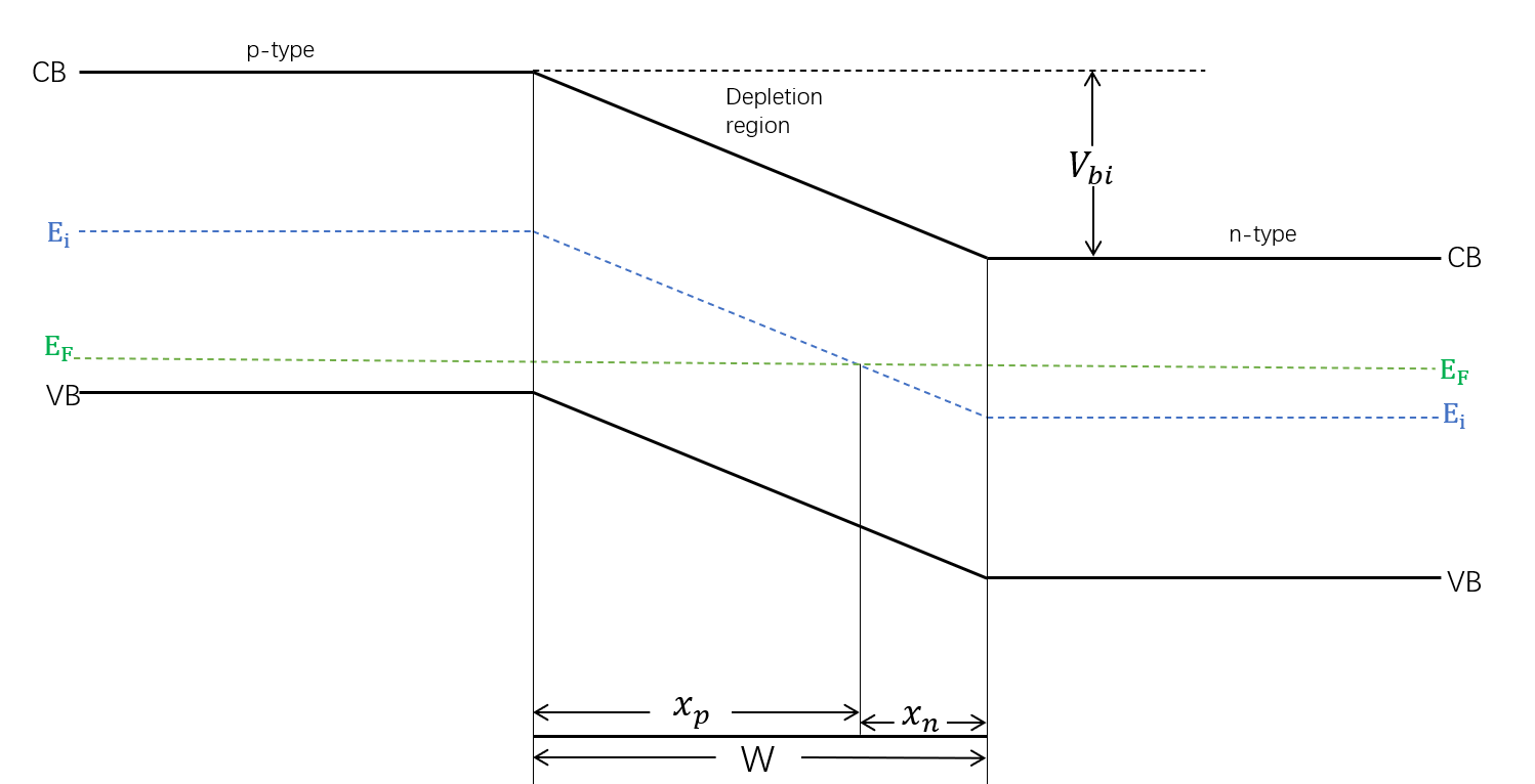
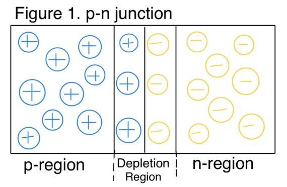
PN junctions are one of the most fundamental physical structures in semiconductor optoelectronics. Their operation is governed by carrier diffusion, drift, depletion region formation, built-in electric fields and electron-hole recombination. This review focuses on the carrier transport and recombination mechanisms in PN junctions and discusses how these mechanisms determine the performance of semiconductor optoelectronic devices. Firstly, the fundamental physics of PN junction formation, energy-band bending and bias-dependent carrier injection is summarized. Then, major transport processes including drift-diffusion transport, minority-carrier injection and doping-dependent current behavior are reviewed. Particular attention is paid to radiative recombination and different types of non-radiative recombination. The review further analyzes the effect of PN junctions in light-emitting diodes, solar cells and photodetectors. Finally, emerging research directions, including heterojunction design, interface passivation, low-dimensional semiconductor junctions and integrated optoelectronic devices, are discussed. This review provides a systematic outline for understanding the relationship between the PN-junction and optoelectronic device performance.
Show more
Read Article PDF
Cite
Research Article Open Access
Multifunctional Aluminum Nitride P-N Diodes Spanning High Voltage and RF Front-End Applications
Article thumbnail
Aluminum nitride (AlN) is distinguished by three outstanding physical properties: an ultra‑wide bandgap, a high critical breakdown electric field, and a substantial piezoelectric effect, making it suitable for extreme-environment electronics and radio frequency (RF) systems. This review focuses on AlN‑based p‑n junction diodes, with emphasis on their application prospects in high‑voltage power switching devices and RF front‑end integration. After reworking the theoretical underpinnings, the paper analyzes the polarization-induced deviation of AlN from standard p-n junction models and the resulting impact on tunneling-assisted carrier transport. At the application level, three directions are then addressed: high‑voltage PIN switches for power grid regulation, solar‑blind ultraviolet (UV) photodetectors for assessing AlN's optoelectronic performance, and bulk acoustic wave (BAW) resonators with monolithic integration into RF front‑end circuits. Fabrication challenges are also considered, particularly ohmic contact formation and surface passivation stability, which emerge as the principal bottlenecks. These bottlenecks pave the way for constructing a strategic roadmap, which provides theoretical perspectives for exploiting AlN's Multiphysics coupling and enables next-generation fully integrated intelligent power and RF microsystems.
Show more
Read Article PDF
Cite
Research Article Open Access
High-Breakdown-Field β-Ga₂O₃ Power FinFETs on Low Cost Bulk Substrates
Article thumbnail
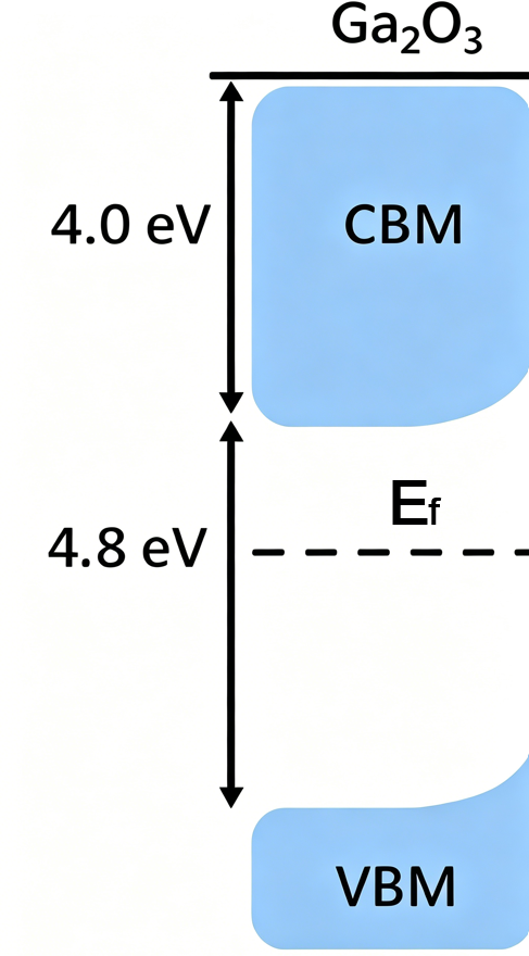
β-Ga₂O₃ has emerged as a promising ultrawide-bandgap semiconductor for next-generation high-voltage power electronics because of its large bandgap, high critical electric field and potential compatibility with low-cost bulk substrates. This review systematically examines recent progress in vertical β-Ga₂O₃ power FinFETs, with emphasis on device physics, electrostatic design, epitaxial growth, fin patterning and thermal management. This article summarizes how three-dimensional gate control and fin geometry enable enhancement-mode operation without relying on p-type doping and compares reported device performance in terms of threshold behavior, breakdown strength and voltage scalability. The review also highlights the complementary roles of HVPE and MOCVD in realizing thick drift layers and low-doped channel regions, as well as the importance of low-damage dry etching in preserving fin sidewall integrity and electrostatic control. Finally, the major limitation of self-heating is discussed together with practical mitigation strategies, including heterogeneous integration, backside heat extraction and interface passivation. Overall, vertical β-Ga₂O₃ FinFETs represent a compelling route toward ultrahigh-voltage power devices, but their practical deployment will depend on coordinated advances in materials growth, process optimization and thermal management.
Show more
Read Article PDF
Cite
Research Article Open Access
Bandgap Engineering of Si-Ge-Sn Alloys for CMOS-Compatible Infrared Optoelectronic Devices
Article thumbnail
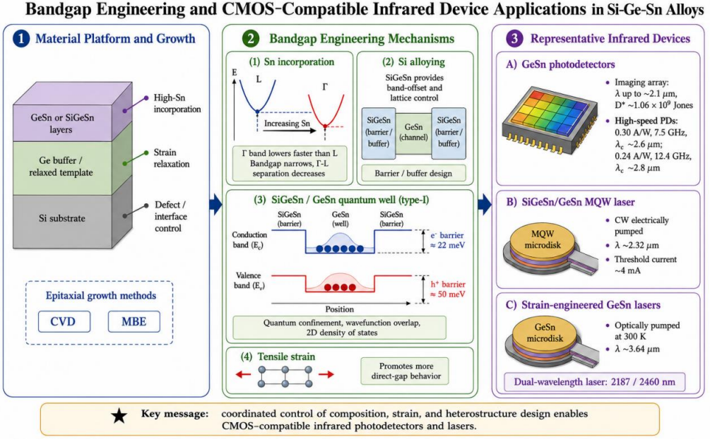
Si-Ge-Sn alloys provide a promising group-IV platform for integrating tunable infrared functions with complementary metal–oxide–semiconductor (CMOS) technology. This review evaluates how epitaxial growth, alloy composition, strain, and heterostructure design influence the electronic structure and device performance of GeSn and SiGeSn materials. Representative experimental and theoretical studies are compared in terms of growth strategy, band alignment, optical response, and reported photodetector and laser characteristics. The reviewed results show that Sn incorporation narrows the GeSn bandgap and lowers the Γ conduction-band valley relative to the L valley, whereas Si alloying mainly adjusts lattice matching and band offsets. Tensile strain and quantum confinement can further enhance direct-gap behavior and carrier overlap. These mechanisms have enabled short-wave infrared photodetectors with multi-gigahertz bandwidth, room-temperature optically pumped GeSn lasers, and electrically pumped SiGeSn/GeSn multiple-quantum-well lasers at cryogenic temperatures. However, device performance remains limited by defect-assisted recombination, dark current, shallow carrier barriers, self-heating, and process non-uniformity. The available evidence therefore indicates that practical Si-Ge-Sn infrared photonics will require the coordinated optimization of epitaxial quality, strain, band alignment, interfaces, and device architecture rather than the independent maximization of Sn content.
Show more
Read Article PDF
Cite