Articles in this Volume

Research Article Open Access
Review of Ultrafast Electron Diffraction Technology
Article thumbnail
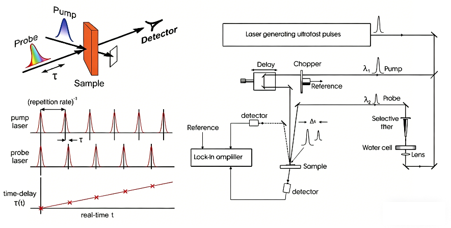
Ultrafast Electron Diffraction (UED), built on the pump‑probe framework, has long been an indispensable tool at the cutting edge of interdisciplinary research spanning physics, chemistry, and biology. Who would have thought that, with its dual advantages of femtosecond temporal resolution and sub‑angstrom spatial resolution, it could directly "visualize" the ultrafast coherent coupling evolution of lattices, electrons, and spins in momentum space? This not only breaks the limitation that traditional spectroscopy can only indirectly infer molecular structural dynamics, but also truly pushes condensed‑matter physics, photochemical reactions, and transient quantum materials into a new era of real‑time atomic‑scale visualization. This paper systematically reviews the landmark breakthroughs of UED in uncovering the microscopic mechanisms of extreme nonequilibrium states of matter, covering phase transition dynamics, electron‑phonon coupling, molecular dynamics, and quantum ultrafast manipulation, fully demonstrating the irreplaceable scientific value of this technology.
Show more
Read Article PDF
Cite
Research Article Open Access
Comparative DC and AC Response of Short-Channel NMOS Test Structures Using the MVS Model and a 65-nm Foundry Model
Article thumbnail
This work presents a compact-model-level comparison between the MIT virtual-source (MVS) model and a 65-nm foundry model for short-channel NMOS devices and simple load-dependent test circuits. A short-channel device schematic based on the MVS concept is first used to establish the physical picture of virtual-source-controlled transport. Two single-transistor test structures are then evaluated: a reference branch without a source resistor and a branch with a source load. Using the provided DC voltage, DC current, and AC frequency-response characteristics, the two models are compared in terms of output-voltage transition, current build-up, and bandwidth roll-off behavior. The results show that both models capture the qualitative impact of loading, but they differ noticeably in the transition location ofVDC, in the low-to-intermediate-bias rise ofIDC, and in the onset of AC roll-off. Under the present test conditions, the MVS model exhibits earlier DC transition, faster current establishment, and a later AC roll-off than the 65-nm foundry model. These observations indicate that a virtual-source-based compact description is not merely an alternative fitting form, but a physically meaningful modeling layer that can influence circuit-level predictions even in very simple transistor test structures.
Show more
Read Article PDF
Cite
Research Article Open Access
TCAD-Based Investigation of Gate Oxide Thickness Effects on SOI- MOSFETs
Article thumbnail
Gate-oxide thickness is a first-order design variable that controls electrostatic coupling, threshold behavior, and leakage in scaled field-effect transistors. This paper presents a compact Silvaco TCAD study of a silicon MOSFET in which the oxide thickness tox is swept from 1 to 5 nm while the drain bias is fixed at VD = 0.05 V. The simulation flow builds the device structure, defines the mesh and regions, assigns material/doping parameters, solves the bias sweep, and extracts transfer characteristics, threshold voltage, and subthreshold swing. The simulated ID-VG curves show a systematic positive shift with increasing tox, indicating weakened gate control. Using the maximum-slope definition of SS and a constant-current threshold criterion of ID = 1 × 10⁻⁷ A, the extracted SS increases from 70.57 to 91.31 mV/dec, while Vth increases from 0.029 to 0.517 V as tox increases from 1 to 5 nm. These results provide a clear TCAD-based visualization of the trade-off between gate dielectric scaling, switching efficiency, and threshold-voltage engineering.
Show more
Read Article PDF
Cite